Our Technical Capability
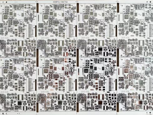
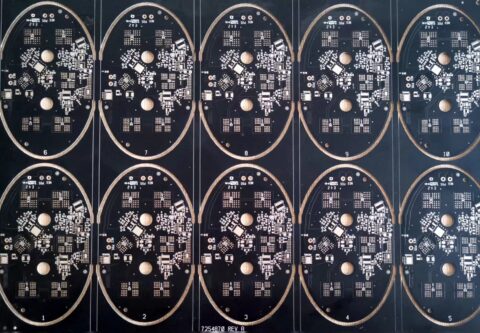
Hosond PCB helps you find the right solution to accomplish any of your PCB product requirements.
Details Of Our Capability
Layers
1-14 layers
Base Material
CEM-3, FR-4, Metal Core, Ceramic
Board Thickness
0.4mm~4.0mm
Min. Hole size
0.2 mm
Copper Weight
1oz ~ 6oz
Min. Line Width/Space
4.0mil/4.0mil
Max. Board Size
620mm✖️920mm
Surface Finishing
HASL-Free, OSP, ENIG, Immersion Tin
Color of Solder Mask
Green, Black, White, Blue, Yellow, Red etc.
Color Of Silkscreen
White, Black etc.

Our Technical Equiptment
Drilling Process
The first-time drilling process is a critical stage in PCB manufacturing where precision holes are drilled into the substrate material to accommodate components and establish electrical connections. This initial drilling is guided by the PCB design layout, which dictates the placement and size of holes for mounting and interconnection purposes. Advanced CNC drilling machines equipped with specialized drill bits ensure accurate hole creation. After drilling, the substrate is often coated with a conductive material, like copper, through processes like electroless copper deposition, creating conductive pathways. The first-time drilling process sets the foundation for subsequent fabrication steps, emphasizing precision and alignment to ensure proper component integration and signal flow in the final assembled circuit board.
Hole Inspection Machine
A hole inspection machine is a specialized equipment utilized in PCB manufacturing to verify the quality and accuracy of drilled holes. This automated system employs optical and imaging technologies to thoroughly examine drilled holes for defects, anomalies, and deviations from design specifications. The machine measures parameters like hole diameter, depth, and alignment, ensuring they meet precise tolerances. It detects issues such as burrs, rough edges, or misalignments that could impact component placement or signal integrity. By automating this crucial inspection process, the hole inspection machine enhances production efficiency , reduces human error, and contributes to the overall reliability and functionality of printed circuit boards. It plays a vital role in maintaining quality control and delivering high-performance PCBs for diverse electronic applications.
Secondary Drilling
Secondary drilling is a crucial process in PCB manufacturing that involves creating additional holes or modifying existing ones after the initial drilling stage. This step is necessary for correcting design errors, accommodating changes in the circuit layout, or facilitating the installation of additional components. Utilizing precision equipment, secondary drilling ensures the precise alignment and placement of holes according to revised specifications. This process enhances the flexibility and adaptability of printed circuit boards, enabling efficient adjustments without the need for complete redesigns.
DES Line
In PCB manufacturing, a Differential Expansion Suppression (DES) line refers to a specialized fabrication technique used to mitigate the potential size variations between different layers of a multilayer PCB during the lamination process. This process involves incorporating materials with controlled thermal expansion coefficients in specific layers, counteracting the dimensional disparities that can arise due to varying heating and cooling rates. The DES line ensures precise alignment and registration of the inner layers, preventing issues such as layer shifting or distortions. By maintaining consistent dimensions, DES lines contribute to the overall reliability and performance of multilayer PCBs, especially in high-density applications where tight tolerances are critical.
V-Cut
At Hosond PCB, we utilize cutting-edge technology and advanced equipment to deliver high-quality printed circuit boards. Among our arsenal of machines, the V-cut machine plays a significant role. The V-cut machine is a precision cutting tool designed specifically to create V-shaped grooves or scores on PCBs. These grooves facilitate easy and precise separation of individual circuit boards during the assembly process. By leveraging the capabilities of the V-cut machine, we ensure clean, accurate, and efficient board separation, resulting in faster production turnaround times and superior quality control. With our commitment to incorporating the latest industry innovations, we harness the power of the V-cut machine to provide exceptional PCB solutions tailored to your specific needs.
Graphic Plating
Graphic plating is a fundamental process in PCB manufacturing that involves the deposition of conductive materials onto specific areas of a circuit board to establish electrical pathways. This technique utilizes photolithography and etching to create intricate patterns on the board’s surface, defining the layout of traces, pads, and vias. A layer of conductive material, often copper, is then electroplated onto these designated regions, enhancing conductivity and connectivity. Graphic plating enables the formation of complex circuitry, enabling the interconnection of electronic components. This precise and controlled method ensures the reliable functionality of the final PCB, making it an essential step in producing high-performance and reliable electronic devices.
Two-dimensional detection
Two-dimensional detection in PCB manufacturing involves the use of advanced imaging systems to inspect printed circuit boards (PCBs) for defects, errors, and anomalies. This technique captures high-resolution images of the PCB’s surface, allowing for thorough analysis sis of components, solder joints, traces, and other critical features. By comparing the obtained images to reference designs or templates, two-dimensional detection can identify issues such as misalignments, soldering problems, bridging, and missing components. This automated inspection process enhances quality control, accelerates production , and ensures consistent adherence to design specifications. Two-dimensional detection is an integral part of modern PCB manufacturing, guaranteeing the reliability and performance of electronic devices across various industries.
Flyingprobe Testing
Flying probe testing is a pivotal quality assurance process in PCB manufacturing. It involves using specialized automated equipment, known as flying probe testers, to assess the integrity and functionality of printed circuit boards. Unlike traditional bed-of-nails testers, flying probe testers employ moving robotic probes that navigate across the board’s surface, executing a series of precise tests. These tests encompass connectivity checks, component verification, and fault detection, ensuring that electrical connections are accurate and components are correctly placed. Flying probe testing is especially advantageous for low-volume production or prototypes due to its flexibility and reduced setup time compared to fixed fixtures. It aids in identifying defects, minimizing production errors, and enhancing product reliability, ultimately contributing to the delivery of high-quality PCBs to various industries.
Testing Machine
A circuit board testing machine is a vital component of PCB manufacturing, ensuring the quality and functionality of printed circuit boards. This automated equipment performs rigorous assessments on PCBs to detect faults, defects, and inaccuracies in electrical connections and component placements. Employing various testing methods such as in-circuit testing (ICT), flying probe testing, and automated optical inspection (AOI), these machines verify the integrity of the board’s design and assembly. They help identify issues early in the production process, minimizing defects and optimizing product reliability. Circuit board testing machines play a crucial role in meeting industry standards, enhancing production efficiency, and delivering high-quality PCBs for a wide range of electronic applications.
Appearance inspection
Automatic Visual Inspection (AVI) is a pivotal quality control process in PCB manufacturing. It employs advanced optical systems and image processing algorithms to automatically scan and analyze printed circuit boards for defects, inconsistencies, and manufacturing errors. AVI technology compares the scanned images to a reference image or design data, identifying issues like soldering defects, misalignments, missing components, or incorrect placements. This automated inspection method enhances production efficiency, reduces human error, and ensures high-quality PCBs. AVI plays a crucial role in maintaining industry standards, minimizing defects, and delivering reliable and defect-free circuit boards for various electronic applications.
Packaging Machine
The packaging process in PCB manufacturing refers to the final assembly and enclosure of the printed circuit board into a protective housing. This step involves integrating the PCB with its associated components, such as microchips, connectors, and passive elements, in accordance with the design specifications. The components are soldered or mounted onto the board’s surface, and any required interconnections are established. Subsequently, the assembled PCB is placed within a protective casing or enclosure, safeguarding it from external elements, mechanical stress, and electromagnetic interference. Proper packaging ensures the durability, functionality, and longevity of the electronic device, making it ready for distribution and use in various applications, from consumer electronics to industrial equipment.
Full-Range PCB
Material Selection
Different base materials achieve specific functions that are used for certain applications such as FR4 offers the advantage of an excellent resistance-to-weight ratio. It remains unaffected by water absorption, maintains high mechanical strength, and demonstrates efficient insulation properties in both dry and humid environments
Our experienced staff can help you select an appropriate material for your business or project requirements.
We also have a mature supply chain that lets us find specific materials for your needs. Through our extensive material selection, you can draw various target audiences to your business.
Our Features & Services
Customizable Color
We can set the color of our PCB products to enhance a specific electric aesthetic. Our extensive selection of color coatings lets you the right color for any project.
Accurate Size and Shape
PCB products need to have the right dimension to fit any electronics or projects. We utilize precise CNC machines to achieve the right board size and shape through our cutting, drilling, polishing, and handcrafting methods.
Various Surface Finishing
We can incorporate various surface finishing onto our PCB products to meet your requirement. With our CNC machining skills and equipment, we can apply different surface finishing options to your PCB products.
Testing
Hosond PCB provides testing method including circuit testing, flying probe testing and AOI (Automated optical inspection)
Packaging Process
Our PCB products can go through different packaging options to increase their durability and service life. Hosond PCB has the experience and equipment to enhance all of our PCB products to address any business requirements.
Tailor-Made for Your Business
Different businesses require specific PCB for their project or product manufacturing needs. Hosond PCB’ customization solution is intended to help your company specifically.
Our experts have the right knowledge and skills to find the right PCB that lets you complete your projects or accomplish any business goals through our complete custom PCB options.
GET A FREE QUOTE
Hassle-Free Service Process
Hosond PCB makes it easy for you to order customized PCB products that meet your specifications accurately.
Get Reliable PCB for Your Brand Boosting
As a PCB manufacturer, we specialize in helping you excel in your fabrication or manufacturing projects. Our commitment lies in delivering high-grade PCBs with exceptional efficiency, ensuring shorter lead times for your convenience. Trust us to provide top-quality solutions tailored to your needs, paving the way for your project’s success.


